Semiconductor wafer defect observer (SBV-20) 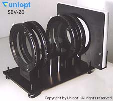
- Overview
Defects occur in semiconductor crystals when the crystal orientation is slightly shifted during pull-up. The defect observer is designed for easy inspection of these defects. It is best suited for inspection of wafers that transmit visible light, such as lithium niobate crystals. It can also be used as an experimental device for photoelasticity.
- Specifications
- Polarizer :150 mm in dimeter
- Observation area: 140 mm in dimeter
- Ovservation method:Cross-micol method, circular polarization method, and other combinations area available.